Thursday, 24 December 2015

MATLAB - Xilinx System Generator - Cont


Xilinx System Generator:

  • Add te xilinx system generator in the simulink window.
  • Add the ports that connect the simulink environmental variables to the xilinx system generator variables.Without those ports both blocks can't be mixed.

  • Select the FPGA device/package
  • Select the program - VHDL/Verilog
  • Generate the project. Then open the project in Xilinx ISE to generate the Programming file.
If you have any questions please email : miycircuits@gmail.com

Wednesday, 23 December 2015

MATLAB - Xilinx System Generator


Xilinx System Generator:

  • Xilinx having simulink related block set on the Xilinx System Generator Software.
  • Install Xilinx System Generator or Latest ISE software.
Settings:


Simulink Window:


  • If both software configured correctly, the xilinx blockset will appear under the Simulink.
If you have any question please email : miycircuits@gmail.com

FPGA Based Electrical Engineering Projects


FPGA Based Electrical Engineering Projects:

FPGA Based SM Speed Control:


FPGA Based Current Control in IM.
FPGA Based NN Based PWM implementation:
FPGA Based Fuzzy Controller Implementation:
Please email us if you have any questions : miycircuits@gmail.com

Tuesday, 22 December 2015

Serial ADC-DAC Implementation in FPGA


ADC-DAC Implementation in FPGA:

Source: Cosmic circuits
  • To test the ADC-DAC read-write logic in FPGA, the above algorithm will be implemented in FPGA.
  • Serial ADC-DAC is considered for the test. 
  • Analog voltage sensed by the ADC is converted in to digital. The digital pattern is written to DAC through FPGA. 
  • DAC - Analog voltage output should be same what ADC sensed @ the input.
ADC Read Operation:
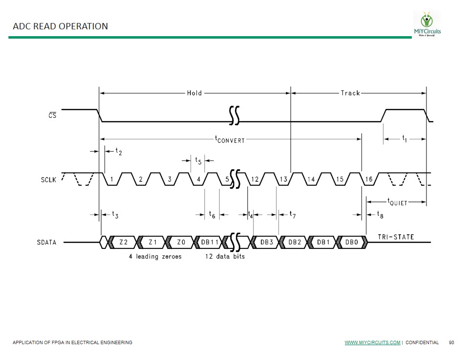
  • When CS selects goes low, the FPGA will start reading the serial data send by the ADC.
DAC Write Operation:


  • When Sync signal goes low, FPGA write the digital data to the DAC. 
Waveforms:

ADC-CS and Serial Data


ADC-Serial Data and Serial Clock


DAC - Sync and Serial Data
  

Check out the below Blog for Job Openings

http://getjob-ad.blogspot.in/

Sunday, 20 December 2015

Class 18 : Multipulse SPWM - Inverter Design


FPGA Based Multipulse SPWM Generation:


  • Multi-pulse generation concept shown above. Carrier and reference signal will be generated in any programming language to find out the number pulse and pulse width in each cycle.

  • Once the pulse width timings are calculated from the program means enter those values in the VHDL code for one cycle and repeat the same for N number of times.

  • Simulation results shows 5 pulse output. 
  • SPWM output probed at the one of the FPGA I/O .it is connected to the inverter MOSFETs through the proper driver circuits.
If you have any questions please email miycircuits@gmail.com

For job opening check out the below blog

http://getjob-ad.blogspot.in/


Friday, 18 December 2015

Class 17 - SPWM Generation - Inverter Control


SPWM Generation - Inverter Control

  • Switches S1,S2,S3,S4,S5,S6 controlled PWM pulses.
  • Because of number of lines on the program is not shown here.
Simulation Results:


  • a1,a2 - on same leg ; similarly b1,b2 ; C1,C2 . a1,a2 generated with 180 deg phase shift.
  • Put_hz - defines the carrier signal frequency
  • put_ff - defines the reference signal frequency that decides the duty and pulse width.
Email us for any questions : miycircuits@gmail.com

For Job Openings Checkout the Below Blog

http://getjob-ad.blogspot.in


Wednesday, 16 December 2015

Class 16 : PID Controller VHDL Program


VHDL Program - Simple PID Controller:


  • Kp,Ki,Kd values are determined through your system(process) to be controlled.
  • The values can be calculated based on conventional calculation or through MATLAB program using the transfer function of the system or converter with PID controller in closed loop.
  • Ref - is actual reference value the system we should achieve @ the output.


  • Error is calculated with reference. 
  • Proportional, Integral and derivative terms are calculated based on the Digital PID equation.
  • Actual control value is calculated P+I+D
  • Controllable error range is 0 to 255. Beyond this range controller reach the saturation.
Simulation Results:


PWM Control:

  • In the given program, only voltage value taken as reference.
Closed Loop PWM control Simulation:


  • In simulation, the pwm pulse widths are getting adjusted when error are beyond acceptable tolerance. check the signal pwm, yout.
If you have any questions please email: miycircuits@gmail.com


Tuesday, 15 December 2015

Class 15 : FPGA - PID Controller Implementation


PID Controller in Converter Design:


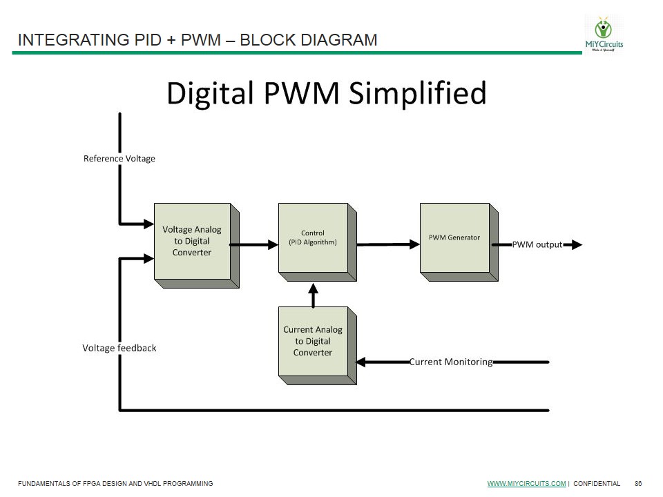
  • In above diagram, Converter output voltage and current is monitored through ADC and it will be compared with desired value (reference). PID controller correct the error value and corresponding PWM pulse width will be adjusted to get desired output.
  • When error zero or in desired range the PID controller will not adjust PWM pulse width.
Analog PID Controller:


Digital PID Controller:

  • Analog and digital PID controller concepts are discussed in text book. Check the theoretical backaround on this.
  • Digital PID controller will be implemented inside the FPGA.

  • Above Digital PID equations will be considered in programming for calculating Proptional, derivative and integrative errors.
Next Class we will be discussing the VHDL program 

If you have any questions please email :miycircuits@gmail.com

Monday, 14 December 2015

Job Opening : Embedded Design Engineer


Company Link : http://technolexis.com/career.html

Job Reference : Indeed

Sunday, 13 December 2015

Class 14 : Motor Speed Control - PWM Control


Motor Speed Control:

  • Simple PWM code is suitable to vary the speed of the motor. 
  • Figure shows the PWM is interfaced through the DC motor through the motor drive.
  • By varying the voltage applied to the DC motor by PWM will change speed.


  • Figure shows the Motor speed control with direction change. 


  • Typical connection from the FPGA development board.
  • Direction and enable(PWM) are the signals driven from the FPGA I/O.
  • It is interfaced to the motor through H-Bridge circuit. VM. Voltage applied to the motor that is controlled through EN (PWM signal)

  • L293 D is the driver circuit cable to drive two 5/12V DC motor. 
  • This principle is applicable for the high voltage DC motor with suitable drive circuit
  • Using Class 12 PWM code the open loop speed control can be implemented. 
If you have any questions please email : miycircuits@gmail.com