
ADC-DAC Implementation in FPGA:

Source: Cosmic circuits
- To test the ADC-DAC read-write logic in FPGA, the above algorithm will be implemented in FPGA.
- Serial ADC-DAC is considered for the test.
- Analog voltage sensed by the ADC is converted in to digital. The digital pattern is written to DAC through FPGA.
- DAC - Analog voltage output should be same what ADC sensed @ the input.
ADC Read Operation:
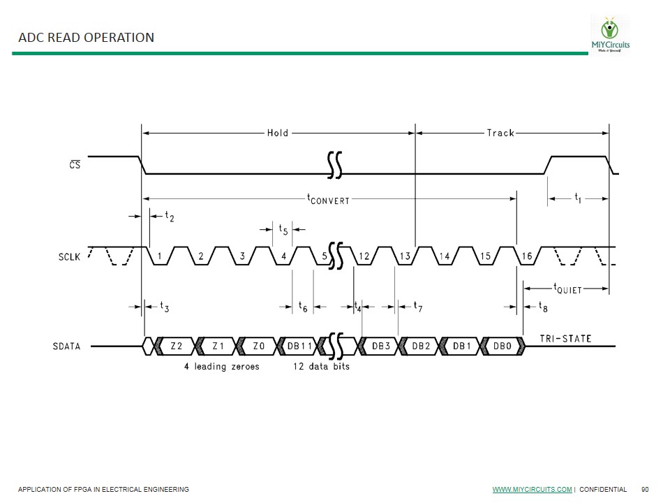
- When CS selects goes low, the FPGA will start reading the serial data send by the ADC.
DAC Write Operation:

- When Sync signal goes low, FPGA write the digital data to the DAC.
Waveforms:
ADC-CS and Serial Data

ADC-Serial Data and Serial Clock

DAC - Sync and Serial Data

Check out the below Blog for Job Openings
http://getjob-ad.blogspot.in/
No comments:
Post a Comment