Thursday 27 August 2015

Switching Regulator - Part 10


Switching Regulator - Reference Design


Simple Buck Converter - Internal FET:

4.5 to 16V Input ; Adjustable output from 0.8V ; Internal MOSFET ;

FIXED pwm frequency ; Soft start

Buck Converter - Internal FET- Programmable SW frequency:

Simple Switcher - External FET:


Step Down Switching regulator - Integrated FET and inductor:

Simple Switcher - External FET and Current protection.


Source : Respective application note

Share your comments. Send your feedback to miycircuits@gmail.com

Saturday 15 August 2015

Switching Regulator - Part 9


Switching Regulator Design: 

Buck Converter:


Selection of PWM controller and parameters:
  • Input voltage range -Design input supply.
  • RT/CLK - Switching frequency and design requirement on Ripple/noise 
  • Enable Pin - Design requirement on power sequencing
  • Soft start - Design requirement on power sequencing and reset release.
  • Vsense - Design requirement on output voltage level.
  • Power Good - Interface to other circuit or indicator
Design:

Input voltage range - 3.5 V to 60V

RT/CLK:

The switching frequency of the TPS54160A is adjustable over a wide range from approximately 100kHz to 2500kHz by placing a resistor on the RT/CLK pin. The RT/CLK pin voltage is typically 0.5V and must have a resistor to ground to set the switching frequency.

Soft start

The slow start capacitor determines the minimum amount of time it will take for the output voltage to reach its nominal programmed value during power up. This is useful if a load requires a controlled voltage slew rate. This is also used if the output capacitance is large and would require large amounts of current to quickly charge the capacitor to the output voltage level.

The slow start time must be long enough to allow the regulator to charge the output capacitor up to the output voltage without drawing excessive current.

Enable Pin:

Many of the common power supply sequencing methods can be implemented using the SS/TR, EN and PWRGD pins. The sequential method can be implemented using an open drain output of a power on reset pin of another device.

The power good is coupled to the EN pin on the device which enables the second power supply once the primary supply reaches regulation. If needed, a 1nF ceramic capacitor on the EN pin of the second power supply provides a desired start-up delay.

Vsense:

The output voltage is set with a resistor divider from the output node to the VSENSE pin. It is recommended to use 1% tolerance or better divider resistors.To improve efficiency at light loads consider using larger value resistors. If the values are too high, the regulator becomes more susceptible to noise and voltage errors from the VSENSE input current are noticeable.

POWER Good:

In general the PWRGD pin is an open drain output. It can be active low or active high output. 

Once the VSENSE pin is between 94% and 107% of the internal voltage reference the PWRGD pin is de-asserted and the pin floats. It is recommended to use a pull-up resistor between the values of 10 and 100kΩ to a voltage source that is 5.5V or less. The PWRGD is in a defined state once the VIN input voltage is greater than 1.5V but with reduced current sinking capability. The PWRGD will achieve full current sinking capability as VIN input voltage approaches 3V. 

The PWRGD pin is pulled low when the VSENSE is lower than 92% or greater than 109% of the nominal internal reference voltage. Also, the PWRGD is pulled low, if the UVLO or thermal shutdown are asserted or the EN pin pulled low.

Source:TI
Share your comments. Send your feedback to miycircuits@gmail.com

Thursday 13 August 2015

Switching Regulator - Part 8


Switching Regulator Selection Parameters:


  • Switching frequency
  • Inductor value, current ratings and DC resistance
  • Filter Capacitor

 Switching frequency

Switching frequency The switching frequency of typical converter ICs on the market is in the range 100 kHz to 2MHz. This leads to the following recommendations:

DESIGN TIP 1: 

Suitable core materials 

Switching frequency < 100 kHz: Iron powder, ferrite, Superflux, WE-PERM 
Switching frequency 100-1000 kHz: Ferrite, Superflux, WE-PERM
Switching frequency > 1000 kHz: Ferrite, WE-PERM

Inductance value 

If there is no application note or software available for the selected PWM controller, inductance can be calculated using the following rule-of-thumb formula:

Buck Converter = > L = (Vinmax - Vout)*(Vout+Vd) /(Vinmax+Vd)*0.3*Iout*f

Boost Convereter => L=(Vout+Vd-Vin min)*Vin*Vin/(2*0.2*Iout*(Vout+Vd)^2*f)

Vout - Desired Output voltage
Vin - Input voltage
Ripple factor - 0.2 to 0.4

DESIGN TIP 2: 

Inductance value
à higher inductance – smaller ripple current 
à lower inductance – higher ripple current The ripple current is essential in determining the core losses. Besides the switching frequency, it is therefore an important parameter for minimising the power loss of the power inductor.


Inductor current ratings

Inductor current ratings The current load for power inductors can be calculated very accurately in terms of DC current load and ripple current load (core losses) using the manufacturers’ simulation software. 

The following approach can be chosen as a rough calculation:

Step-down regulator: Nominal current of the inductor: In = Iout Maximum coil current: Imax = 1.5 x In Step-up regulator: Nominal current of the inductor: In = (Vout/Vin) Iout Maximum coil current: I max = 2 x In

DESIGN TIP 3:

The nominal current for power inductors is usually linked to the specified self-heating with DC current – here self-heating of +40°C is common at the nominal current. According to semiconductor manufacturers‘ recommendations, the saturation current is the point at which the inductance value has fallen by 10%. Unfortunately, this is not a standard value for power inductor data sheet specifications and often leads to misinterpretation among users.

DC resistance:

Once the required values for inductance L and inductor currents are calculated, you select a power inductor with the minimum possible DC resistance. Here the demands are often counteractive: Small size, high energy storage density and low DC resistance.

DESIGN TIP 4: 

DC resistance with the same size 

  •  higher inductance – higher DC resistance
  • lower inductance – lower DC resistance 
  • same inductance for a shielded inductor – lower DC resistance The DC resistance is essential in determining the wire heating losses; this is another important parameter for minimizing the power loss of the power inductor.

Type and EMC

Magnetic shielded power inductors are recommended for EMC-critical applications. The shielding prevents uncontrolled magnetic coupling of the windings with neighbouring conductor tracks or components.

DESIGN TIP 5: 

Use a magnetically shielded power inductor if at all possible. Do not route any conductor tracks under the component and do not place any circuit boards directly above the component, as this could give rise to coupling via the air gap remaining.

DESIGN TIP 6:

Advantage of magnetically shielded inductors of the same type:
à higher AL value, therefore lower DC resistances for the same inductance = lower wire losses. 

Disadvantage of magnetically shielded inductors of the same type:
à slightly increased core losses due to a larger core volume. Given correct dimensioning the core losses remain low.

Output L-C filter An L-C filter at the DC converter output is recommended if a low noise output voltage is required. The components can be selected as follows


DESIGN TIP 7: 

  • Select cut-off frequency at 1/10 of the switching regulator frequency 
  • Select output capacitor (e.g. 22 µF) 
  • Calculate inductance L = 1/ (2 • π • f)^2 • C
DESIGN TIP 8:

Ripple measurements To properly measure ripple on either input or output of a switching regulator, a proper ring in Tipp measurement is required. Standard oscilloscope probes come with a grounding clip, or a long wire with an alligator clip. Unfortunately, for high frequency measurements, this ground clip can pick-up high frequency noise and erroneously inject it into the measured output ripple. The standard evaluation board accommodates a home made version by providing probe points for both the input and output supplies and their respective grounds. This requires the removing of the oscilloscope probe sheath and ground clip from a standard oscilloscope probe and wrapping a non-shielded bus wire around the oscilloscope probe. If there does not happen to be any non shielded bus wire immediately available, the leads from axial resistors will work. By maintaining the shortest possible ground lengths on the oscilloscope probe, true ripple measurements can be obtained.

Source:Digikey AN


Share your comments. Send your feedback to miycircuits@gmail.com

Monday 10 August 2015

Switching Regulator - Part 7


Switching Regulator Types:

Basic components in the Switching regulator is
  • Inductor -Storage element
  • Capacitor - Filtering element
  • Switch - Controls the power transferred to Output
Placement of the storage elements in reference to the switching elements and their quantities generally determines the type of switching supply configuration.

Buck Converter: 


It is also known as step down converter. It is most commonly used switching regulator. It is used to lower the input dc voltage. The output dc voltage always less than input dc voltage.

Boost Converter:


It is also known as step up converter. The output DC voltage is higher than the input DC voltage. Linear regulators cannot produce this feature.

Buck-Boost Converter:


The buck-boost or inverting regulator produces a dc voltage that's above,below, or opposite in polarity to the input.

SEPIC Converter:


The single ended primary inductor converter is similar to a traditional buck-boost converter. The output voltage can be greater than, less than or equal to the input voltage. This converter also capable of true shutdown. When switch is off the output voltage is zero.

CUK Converter:


The CUK converter’s output voltage can be greater than or less than the input voltage magnitude.It uses a capacitor as its main energy-storage component. By using inductors on the input and output, the CUK converter produces very little input and output current ripple. And, it has minimized electromagnetic interference (EMI) radiation.

Charge Pump:


The switched capacitor regulator uses capacitors as energy storage elements to create a higher or lower voltage. It can generate arbitrary voltages, depending on the controller and circuit topology. Charge pumps can double, triple, halve, invert, or fractionally multiply or scale voltages such as x3/2, x4/3, and x2/3. It also can provide multiple outputs.

Flyback Converter:


The flyback converter is the most versatile of all the topologies. It allows for one or more output voltages, some of which may be opposite in polarity. Additionally, it is very popular in battery-powered systems. It provides isolation as well.
Forward converter:
The forward converter is a buck regulator with a transformer inserted between the buck switch and the load. It provides both higher and lower voltage outputs as well as isolation. It also might be more energy efficient than a flyback converter.
Push-Pull Converter:
The push-pull converter is a forward converter with two primaries . It can generate multiple output voltages, some of which may be negative in polarity. It provides isolation as well. However, it requires very good matching of the switch transistors to prevent unequal ON times.
Half-bridge Converter:
The half-bridge converter is usually operated directly from the ac line. The switch transistor drive circuitry must be isolated from the transistors, requiring the use of base drive transformers.
Full-bridge Converter:
The full-bridge converter provides isolation from the ac line. The pulse-width modulation (PWM) control circuitry is referenced to the output ground, requiring a dedicated voltage rail to run the control circuits. The base drive voltages for the switch transistors have to be transformer-coupled because of the required isolation

Source:ElectronicDesign
Share your comments. Send your feedback to miycircuits@gmail.com

Friday 7 August 2015

Switching Regulator - Part 6


Switching Regulator Layout Checklist:


1. Plan of the Layout

1.0 Understand the system mechanical and thermal constraints. Save sufficient board real estate/area          for power supply in the beginning/planning stage of the big system. Don’t wait to do it as the last       step.

1.1 Power supply output capacitors are located physically close to the supply load.
       – To minimize impedance between the output capacitors and the fast transient load.

1.2   Locate power supply near cooling fan; ensure good air flow path.
       – For optimal cooling of the power supply.

1.3 Ground layer is placed between the power layer and the small signal layer.
       – To return the current from the power component layer and to shield sensitive small signal                traces from power stage switching noise.

1.4 Highlight the schematic traces to identify high current traces, noisy traces and sensitive small             signal traces.

1.5 Decide the components on top and bottom sides of the PCB board. Try to keep all power                     components on the same side.

2. Power Stage Layout

2.1 Place the power components first. Please them in the way that minimizes the length of the high        current flow paths through input capacitors, power FETs, inductors, RSENSE and output                     capacitors.
       – To minimize the PCB impedance and conduction losses on high current paths.

2.2 Have solid, low impedance land patterns for the power components, including capacitors, FETs,      diodes, inductors and current sensing resistors. Use large copper plane for VIN, VOUT and GND
      – To minimize the trace impedance and power component thermal stress.

2.3 Use thick copper or multiple layers for high current power layers.
      – To minimize the PCB conduction loss and reduce thermal stress.

2.4 If it is necessary to route a power trace to another layer, choose a trace in low di/dt paths and use       multiple vias for interconnection.
      – To minimize noise propagation and connection impedance between layers.

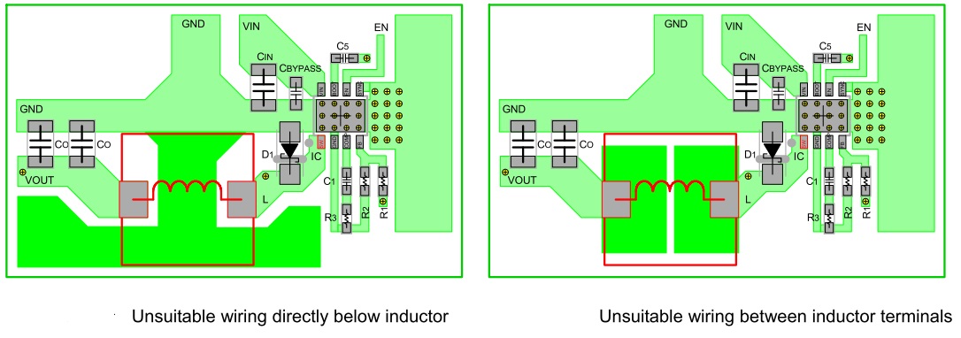
2.5 Minimize the pulsating current loop area.
      – To minimize the pulsating loop (hot loop) inductance and absorb switching noise.

2.6 Minimize and isolate/shield the high dv/dt SW node areas.
      – To minimize the EMI noise source from the high dv/dt SW nodes.

2.7 Separate input current paths among supplies if there is more than one supply on the same input         rail and the supplies are not synchronized. Have local input decoupling capacitor for each                   supply.
      – To avoid common impedance noise coupling among supplies.

2.8 PolyPhase converter. Try to have symmetric layout for each phase. Have local ceramic                         decoupling capacitor for each phase.

3. Control Circuit Layout

3.1 Locate the control circuitry in a quiet location that is close to output capacitors or input                     capacitors.
    – To minimize the noise to the control circuitry.

3.2 Use a separate SGND ground island for the components to the following small signal pins:
       – To minimize the noise to the control circuitry.
3.3 Use PGND for power.

3.4 Has a single connection point between SGND and PGND. One suggested location is underneath          the IC.
       – To minimize SGND noise and provide low impedance gate driver current return path.

3.5 To minimize the connection impedance and provide best noise decoupling with HF capacitors.

3.6 Current sensing traces – Kelvin sensing is required with closely routed sense signals

3.7 Remote voltage sensing traces should be routed together with a pair of traces.
     – To minimize the noise and sensing error.

3.8 Gate driver traces – TG and SW traces should be routed together with minimum loop area                   minimize the noise source from the high dv/dt gate driver traces.

3.9 Maintain distance between sensitive small signal traces and noisy traces/planes.
     – To minimize the capacitive noise coupling between noisy traces and small signal traces.

3.10 Trace width –Maintain the trace width as required.
       – To minimize the trace impedance.

Source: Linear

Thursday 6 August 2015

Switching Regulator - Part 5


Switching Regulator Layout Guideline:

Converter Current Loop and field:


Few Layout Guideline on the converter routing:
  • Place input capacitor and free-wheel diode on the same PCB surface layer as the IC terminal and as close as possible to IC.
  • Include thermal via if necessary to improve heat dissipation.
  • Place inductor close to IC, no need to be as close as input capacitor. This is to minimize radiation noise from the switching node and do not expand copper area more than needed.
  • Place output capacitor close to inductor.
  • Keep wiring of return path away from noise causing areas, such as inductor and diode.

Placing of input Capacitor and Free-wheel Diode
  • Place CBYPASS near IC terminal on the top layer. Large capacitance capacitor CIN can be separated about 2cm from CBYPASS that supplies most of the pulse-current.
  • When difficulty in space occupied, and if cannot place CIN on the same surface as IC, it can be placed at the bottom layer through via. Risks regarding noise can be avoided with this, but there is a possibility of ripple-voltage to increase at high-current, influenced by via resistance.
  •  Voltage noise is created by inductance of the via, and the bypass capacitor operates as a reverse effect. Do not carry out this kind of layout design.
  • In case of buck converter, high frequency of several hundred MHz will be loaded to the ground of CIN even with CBYPASS placed close to IC. Therefore placing ground of CIN and CO must be separated from each other by at least 1cm to 2cm.
  • Free-wheel diode D must be placed closer and on same surface of IC terminal. With long distance between IC terminal and diode, the spike noise will be induced due to wiring inductance
  • Use short and wide wiring for free-wheel diode, and connect directly to GND terminal and switching terminal of IC.
  • Do not place it on bottom surface layer through via, as noise will be worse, which is influenced by via inductance.
  • Wiring inductance increases due to distance between diode and switching terminal, and GND terminal of IC and spike noise gets higher.
  •  To improve spike noise caused by unsuitable layout the RC snubber-circuit may be added as a countermeasure. This snubber-circuit must be placed closer to switching terminal and GND terminal of IC. Placing it at the both ends of diode will not absorb spike noise generated by wiring inductance.


Introduce Thermal Via
  • Copper area of PCB contributes to heat dissipation, but because it does not have enough thickness, the heat dissipation result that meets area cannot be achieved from limited PCB size. Heat is dissipated using base material of board as a radiator. To deliver heat to opposite layer of the board efficiently and to highly reduce heat resistance, the thermal via are introduced.

Placing Inductor
  • Place inductor close to IC, no need to place it as close as the input capacitor, to minimize radiation noise from switching node, and do not expand copper pattern area if not necessary.
  • Increasing copper area is most likely to be thought of to improve wire resistance and to cool down device, but enlarged area may work as an antenna and may lead to increase in EMI.
  • Not placing ground layer directly below the inductor is also a point to pay attention to, when placing inductor. Due to the eddy current occurring in the ground layer, the inductor value decreases and the loss increases (decrease of Q) with set-off effect from line of magnetic force.
  • Signal line other than ground also has the possibility of propagating switching noise caused by eddy current. It is better to avoid wiring directly under inductor. If wiring is unavoidable, please use closed magnetic circuit structured inductor with small leak from line of magnetic force.
  • Space between inductor terminals must also be paid attention. If distance between terminals are close, high frequency signal of switching node is induced to output through stray capacitance.


Place Output Capacitor Close to Inductor
  • Output current is smooth in buck converter as inductor is inserted to output in series. Place output capacitor close to inductor; no need to place it as close as input capacitor
  • High frequency of several hundred MHz is loaded on ground of input, so placing ground of CIN and COUT 1cm to 2cm apart is recommended. If they are close to each other, high frequency noise of input may be propagated to output through COUT.
 Feedback Route

  • Feedback signal route is a wire which needs most attention in signal wiring. If this wire has noise, an error will occur in output voltage and the operation will become unstable.
  • Feedback terminal of IC which inputs feedback signal, is normally designed with high impedance. Output of this terminal and resistor crossover network must be connected with short wire.
  • Part which detects the output voltage must be connected after output capacitor or at both ends of output capacitor.
  • Wiring the resistor-divider circuit nearby and parallel, makes it better for noise tolerance.
  •  Draw wire far away from switching node of inductor and diode. Do not wire directly below the inductor and diode, and not parallel to power supply line. Multilayer board must be also wired in the same way.
  • Transfer the feedback route to bottom layer of PCB through via, and the layout away from the switching node.. In this case, noise is induced to feedback route by magnetic field generated around the inductor.
       
Ground

  • Analog small-signal ground and power-ground must be isolated.
  • Power-ground without separating from top layer is very ideal. Connecting isolated power-ground on bottom layer through via causes losses and aggravate the noise due to the effect of inductance and resistance of via.
  • Providing ground plane in PCB inner layer and bottom layer is to reduce and shield DC loss, and to radiate heat better, but it is only a supplementary ground.
  • When placing ground plane on bottom layer, and in PCB inner-layers of a multilayer board, connection of input power-ground and the ground for free-wheel diode with high frequency switching noise, must be taken care.
  • Power-ground plane in 2nd layer to reduce losses, connect top layer and 2nd layer with many via and reduce impedance of power-ground.


Source : ROHM AN
         
Share your comments. Send your feedback to miycircuits@gmail.com

Wednesday 5 August 2015

Switching Regulator - Part 4


Boost Converter:

Simple circuit diagram:


boost converter (step-up converter) is a DC-to-DC power converter with an output voltage greater than its input voltage.

Operation:

Basic Elements DC source, Switch, inductor,capacitor,Diode and PWM controller. PWM controller controls switch ON/OFF timings.

MOSFET ON Condition:

  1. MOSFET is Short
  2. Diode is Reverse biased. Blocks the current flow
  3. Current flow path DC Source (+) --> Inductor -->MOSFET --> Source (-)
  4. Inductor stores the energy on this cycle. (Magnetic field action)
MOSFET OFF Condition:


During OFF condition, 

  1. MOSFET is Open
  2. Diode is forward biased
  3. Current flow path DC Source (+)--> Inductor --> Diode --> Capacitor and Load --Source(-)
  4. Inductor dissipates the energy on this cycle. (Magnetic field action)
  5. Capacitors stores the energy. (Charging)

Next ON Cycle:


  1. MOSFET is Short
  2. Diode is Reverse biased. Blocks the current flow
  3. Current flow path DC Source (+) --> Inductor -->MOSFET --> Source (-)
  4. Another current path: Stored capacitor --> Load -- Source (-)
  5. Inductor stores the energy on this cycle. (Magnetic field action)
  6. Capacitor dissipates the energy to a load
DC output is depends on the 
  1. DC input voltage
  2. Duty cycle (0 to 100 %)
  3. Switching frequency
  4. Inductor and capacitor selection
Typical power boost converter -Low power application:


Share your comments. Send your feedback to miycircuits@gmail.com

Monday 3 August 2015

Switching Regulator - Part 3


Buck Converter:

Simple Circuit Diagram:


  1. VOUT < Vin
  2. Efficiency > 90%
  3. Power MOSFET may be internal or External for PWM controller
Detailed circuit Diagram:


  1. Adding Large C across the load to control ripple.
  2. Adding a inductor,to prevent the huge current spike
  3. Adding Free wheeling diode, the switch can open and the inductor current can continue to flow.
Discontinuous operation:


  1. Occurs for light loads, or low operating frequencies, where the inductor current eventually hits zero during the switch-open state
  2. The diode opens to prevent backward current flow
  3. The small capacitances of the MOSFET and diode, acting in parallel with each other as a net parasitic capacitance, interact with L to produce an oscillation
  4. The output C is in series with the net parasitic capacitance, but C is so large that it can be ignored in the oscillation phenomenon


Typical Industry Step-down Converter:


Share your comments. Send your feedback to miycircuits@gmail.com

Sunday 2 August 2015

Switching Regulator -Part 2


Switching Regulator - Switcher


  1. Switching converters are often referred to as Switchers
  2. Conversion is based on the inductive storage and filtering methods
  3. Basic elements in the switchers are voltage source, Switch,inductor,capacitor,Diode
  4. Output voltage ripple depends on the inductor, capacitor and switching frequency
  5. Ideal efficiency is 100 % (lossless elements)
  6. Typical efficiency 90% +
Major differentiating points as compared to LDOs
  1. Wide Input voltage range (Vin)
  2. High Efficiency (> 90%)
  3. Compact in size when comparing with same output power
  4. Multiple phase and multiple outputs
Most widely used Switching Regulators 
  1. Buck Converter
  2. Boost Converter
  3. Buck-Boost Converter
  4. Fly-back Converter