
Switching Regulator Layout Guideline:
Converter Current Loop and field:


Few Layout Guideline on the converter routing:
- Place input capacitor and free-wheel diode on the same PCB surface layer as the IC terminal and as close as possible to IC.
- Include thermal via if necessary to improve heat dissipation.
- Place inductor close to IC, no need to be as close as input capacitor. This is to minimize radiation noise from the switching node and do not expand copper area more than needed.
- Place output capacitor close to inductor.
- Keep wiring of return path away from noise causing areas, such as inductor and diode.
Placing of input
Capacitor and Free-wheel Diode
- Place CBYPASS near IC terminal on the top layer. Large capacitance capacitor CIN can be separated about 2cm from CBYPASS that supplies most of the pulse-current.
- When difficulty in space occupied, and if cannot place CIN on the same surface as IC, it can be placed at the bottom layer through via. Risks regarding noise can be avoided with this, but there is a possibility of ripple-voltage to increase at high-current, influenced by via resistance.
- Voltage noise is created by inductance of the via, and the bypass capacitor operates as a reverse effect. Do not carry out this kind of layout design.
- In case of buck converter, high frequency of several hundred MHz will be loaded to the ground of CIN even with CBYPASS placed close to IC. Therefore placing ground of CIN and CO must be separated from each other by at least 1cm to 2cm.
- Free-wheel diode D must be placed closer and on same surface of IC terminal. With long distance between IC terminal and diode, the spike noise will be induced due to wiring inductance
- Use short and wide wiring for free-wheel diode, and connect directly to GND terminal and switching terminal of IC.
- Do not place it on bottom surface layer through via, as noise will be worse, which is influenced by via inductance.
- Wiring inductance increases due to distance between diode and switching terminal, and GND terminal of IC and spike noise gets higher.
- To improve spike noise caused by unsuitable layout the RC snubber-circuit may be added as a countermeasure. This snubber-circuit must be placed closer to switching terminal and GND terminal of IC. Placing it at the both ends of diode will not absorb spike noise generated by wiring inductance.


Introduce Thermal
Via

- Copper area of PCB contributes to heat dissipation, but because it does not have enough thickness, the heat dissipation result that meets area cannot be achieved from limited PCB size. Heat is dissipated using base material of board as a radiator. To deliver heat to opposite layer of the board efficiently and to highly reduce heat resistance, the thermal via are introduced.
Placing Inductor
- Place inductor close to IC, no need to place it as close as the input capacitor, to minimize radiation noise from switching node, and do not expand copper pattern area if not necessary.
- Increasing copper area is most likely to be thought of to improve wire resistance and to cool down device, but enlarged area may work as an antenna and may lead to increase in EMI.
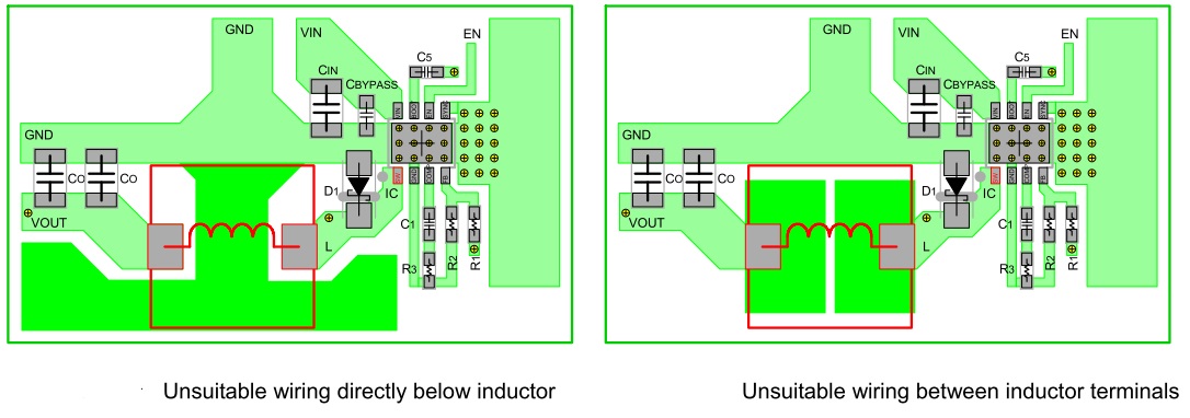
- Not placing ground layer directly below the inductor is also a point to pay attention to, when placing inductor. Due to the eddy current occurring in the ground layer, the inductor value decreases and the loss increases (decrease of Q) with set-off effect from line of magnetic force.
- Signal line other than ground also has the possibility of propagating switching noise caused by eddy current. It is better to avoid wiring directly under inductor. If wiring is unavoidable, please use closed magnetic circuit structured inductor with small leak from line of magnetic force.
- Space between inductor terminals must also be paid attention. If distance between terminals are close, high frequency signal of switching node is induced to output through stray capacitance.

Place Output
Capacitor Close to Inductor
- Output current is smooth in buck converter as inductor is inserted to output in series. Place output capacitor close to inductor; no need to place it as close as input capacitor
- High frequency of several hundred MHz is loaded on ground of input, so placing ground of CIN and COUT 1cm to 2cm apart is recommended. If they are close to each other, high frequency noise of input may be propagated to output through COUT.
Feedback Route
- Feedback signal route is a wire which needs most attention in signal wiring. If this wire has noise, an error will occur in output voltage and the operation will become unstable.
- Feedback terminal of IC which inputs feedback signal, is normally designed with high impedance. Output of this terminal and resistor crossover network must be connected with short wire.
- Part which detects the output voltage must be connected after output capacitor or at both ends of output capacitor.
- Wiring the resistor-divider circuit nearby and parallel, makes it better for noise tolerance.
- Draw wire far away from switching node of inductor and diode. Do not wire directly below the inductor and diode, and not parallel to power supply line. Multilayer board must be also wired in the same way.
- Transfer the feedback route to bottom layer of PCB through via, and the layout away from the switching node.. In this case, noise is induced to feedback route by magnetic field generated around the inductor.

Ground
- Analog small-signal ground and power-ground must be isolated.
- Power-ground without separating from top layer is very ideal. Connecting isolated power-ground on bottom layer through via causes losses and aggravate the noise due to the effect of inductance and resistance of via.
- Providing ground plane in PCB inner layer and bottom layer is to reduce and shield DC loss, and to radiate heat better, but it is only a supplementary ground.
- When placing ground plane on bottom layer, and in PCB inner-layers of a multilayer board, connection of input power-ground and the ground for free-wheel diode with high frequency switching noise, must be taken care.
- Power-ground plane in 2nd layer to reduce losses, connect top layer and 2nd layer with many via and reduce impedance of power-ground.


Source : ROHM AN
Share your comments.
Send your feedback to miycircuits@gmail.com
No comments:
Post a Comment