Wednesday, 30 December 2015

Class 05: PCB - Aspect Ratio, Solder Mask, Silk Screen


Aspect Ratio, Solder Mask, Silk Screen:

  • Aspect ratio one of the parameter to decide the PCB board thickness.
  • If board using small diameter and board thickness is more means the aspect ratio range may not met and PCB is not manufacturable. 


  • Solder Mask protect the circuits (Copper) from oxidation and accidental short and shock to the human.
  • In general, most of the PCB using the Green color solder mask. Now a days solder mask available in the black, red and blue color also.

  • Surface finish is coat over the exposed conductor. In general, coat over the pads of the components, coat over gold finger etc. (Coat over the exposed copper). 
  • Gold finish is used for the high speed circuits/signals.


  • Silkscreen is reference of the components on the board.
  • Mainly it is used to identify the design components in the PCB, Connector pin orientation, diode and tantalum/bulk capacitor,DC power Jack orientation, etc.
If you have any questions please email: miycircuits@gmail.com


Tuesday, 29 December 2015

Class04: PCB Manufacturing Method


PCB Manufacturing Method:


  • Photomask generated from the gerber file. 
  • Circuit pattern will be applied over the copper foil through photosensitive material.


  • Etching step remove the copper that is not the part of the circuit.

  • Milling is another method to remove the unwanted copper.

  • Once etching completed, vias will be made using drilling bits based on via diameter.
  • Now a days, vias with small diameter is made using laser.

Monday, 28 December 2015

Class03 : PCB Material


PCB Material:


  • Core - Copper foil layer @ both side of the insulating material. 
  • It is available on standard thickness and size.


  • Copper conductors are available on the standard thickness. 
  • 2oz copper is used for high current application. 

  • Core Insulators are standard dielectric material.Most commonly used one is FR4.
  • For high speed application and high temperature resistant the suitable material can be selected.

Saturday, 26 December 2015

Class02- Printed Circuit Board -PCB


Printed Circuit Board (PCB)

What is PCB ?
PCB Design Process: 
  • PCB Design Process

    • PCB Layout and Schematic Tool Library Creation based on the design
    • Schematic Entry
    • Netlist Export
    • Layout 
    • Gerber Generation
    • CAM and Manufacturing Check
    • PCB Fabrication

  • What is Gerber

PCB Assembly Structure:


  • Major Structure in PCB
    • PCB Core
    • Dielectric Material
    • PCB Copper Layer
    • Circuit Layer
    • Solder Paste
    • Solder Mask
    • Silk Screen

If you have any questions please email to miycircuits@gmail.com

Class 01 - High Speed Board Design Techniques


Tutorial on High Speed Board Design Techniques 


  • In this tutorial the following topics will be discussed
    • PCB manufacturing process
    • PCB Design terminology
    • Signal Transmission
    • Differential Signalling 
    • Signal Integrity
    • PCB Layout Rule for Signal Integrity
    • Constraint Manager and PCB Layout Checklist


Friday, 25 December 2015

Welcome to High Speed Board design Class !


FPGA in Electrical Engineering: 

The High Speed Design Classes are starting tomorrow.

The Following topics will be covered


  • PCB Manufacturing methods
  • PCB terminology
  • Signal Transmission
  • Differential transmission
  • Signal Integrity
  • Layout Techniques for signal integrity reduction
  • Constraint Manager and high Layout review techniques
Follows us on Google plus to get an Update.


Thursday, 24 December 2015

MATLAB - Xilinx System Generator - Cont


Xilinx System Generator:

  • Add te xilinx system generator in the simulink window.
  • Add the ports that connect the simulink environmental variables to the xilinx system generator variables.Without those ports both blocks can't be mixed.

  • Select the FPGA device/package
  • Select the program - VHDL/Verilog
  • Generate the project. Then open the project in Xilinx ISE to generate the Programming file.
If you have any questions please email : miycircuits@gmail.com

Wednesday, 23 December 2015

MATLAB - Xilinx System Generator


Xilinx System Generator:

  • Xilinx having simulink related block set on the Xilinx System Generator Software.
  • Install Xilinx System Generator or Latest ISE software.
Settings:


Simulink Window:


  • If both software configured correctly, the xilinx blockset will appear under the Simulink.
If you have any question please email : miycircuits@gmail.com

FPGA Based Electrical Engineering Projects


FPGA Based Electrical Engineering Projects:

FPGA Based SM Speed Control:


FPGA Based Current Control in IM.
FPGA Based NN Based PWM implementation:
FPGA Based Fuzzy Controller Implementation:
Please email us if you have any questions : miycircuits@gmail.com

Tuesday, 22 December 2015

Serial ADC-DAC Implementation in FPGA


ADC-DAC Implementation in FPGA:

Source: Cosmic circuits
  • To test the ADC-DAC read-write logic in FPGA, the above algorithm will be implemented in FPGA.
  • Serial ADC-DAC is considered for the test. 
  • Analog voltage sensed by the ADC is converted in to digital. The digital pattern is written to DAC through FPGA. 
  • DAC - Analog voltage output should be same what ADC sensed @ the input.
ADC Read Operation:
  • When CS selects goes low, the FPGA will start reading the serial data send by the ADC.
DAC Write Operation:


  • When Sync signal goes low, FPGA write the digital data to the DAC. 
Waveforms:

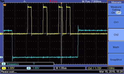
ADC-CS and Serial Data


ADC-Serial Data and Serial Clock


DAC - Sync and Serial Data
  

Check out the below Blog for Job Openings

http://getjob-ad.blogspot.in/

Sunday, 20 December 2015

Class 18 : Multipulse SPWM - Inverter Design


FPGA Based Multipulse SPWM Generation:


  • Multi-pulse generation concept shown above. Carrier and reference signal will be generated in any programming language to find out the number pulse and pulse width in each cycle.

  • Once the pulse width timings are calculated from the program means enter those values in the VHDL code for one cycle and repeat the same for N number of times.

  • Simulation results shows 5 pulse output. 
  • SPWM output probed at the one of the FPGA I/O .it is connected to the inverter MOSFETs through the proper driver circuits.
If you have any questions please email miycircuits@gmail.com

For job opening check out the below blog

http://getjob-ad.blogspot.in/


Friday, 18 December 2015

Class 17 - SPWM Generation - Inverter Control


SPWM Generation - Inverter Control

  • Switches S1,S2,S3,S4,S5,S6 controlled PWM pulses.
  • Because of number of lines on the program is not shown here.
Simulation Results:


  • a1,a2 - on same leg ; similarly b1,b2 ; C1,C2 . a1,a2 generated with 180 deg phase shift.
  • Put_hz - defines the carrier signal frequency
  • put_ff - defines the reference signal frequency that decides the duty and pulse width.
Email us for any questions : miycircuits@gmail.com

For Job Openings Checkout the Below Blog

http://getjob-ad.blogspot.in


Wednesday, 16 December 2015

Class 16 : PID Controller VHDL Program


VHDL Program - Simple PID Controller:


  • Kp,Ki,Kd values are determined through your system(process) to be controlled.
  • The values can be calculated based on conventional calculation or through MATLAB program using the transfer function of the system or converter with PID controller in closed loop.
  • Ref - is actual reference value the system we should achieve @ the output.


  • Error is calculated with reference. 
  • Proportional, Integral and derivative terms are calculated based on the Digital PID equation.
  • Actual control value is calculated P+I+D
  • Controllable error range is 0 to 255. Beyond this range controller reach the saturation.
Simulation Results:


PWM Control:

  • In the given program, only voltage value taken as reference.
Closed Loop PWM control Simulation:


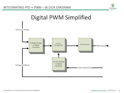
  • In simulation, the pwm pulse widths are getting adjusted when error are beyond acceptable tolerance. check the signal pwm, yout.
If you have any questions please email: miycircuits@gmail.com